
World’s First: Kyocera and Tohoku University Develop Technology to Integrate Optical Isolators Directly onto Silicon Photonics Chips*1
Kyocera Corporation (President: Shiro Sakushima; "Kyocera") and the Research Institute of Electrical Communication (RIEC), Tohoku University (Director: Kazushi Ishiyama; "Tohoku University") have deve...
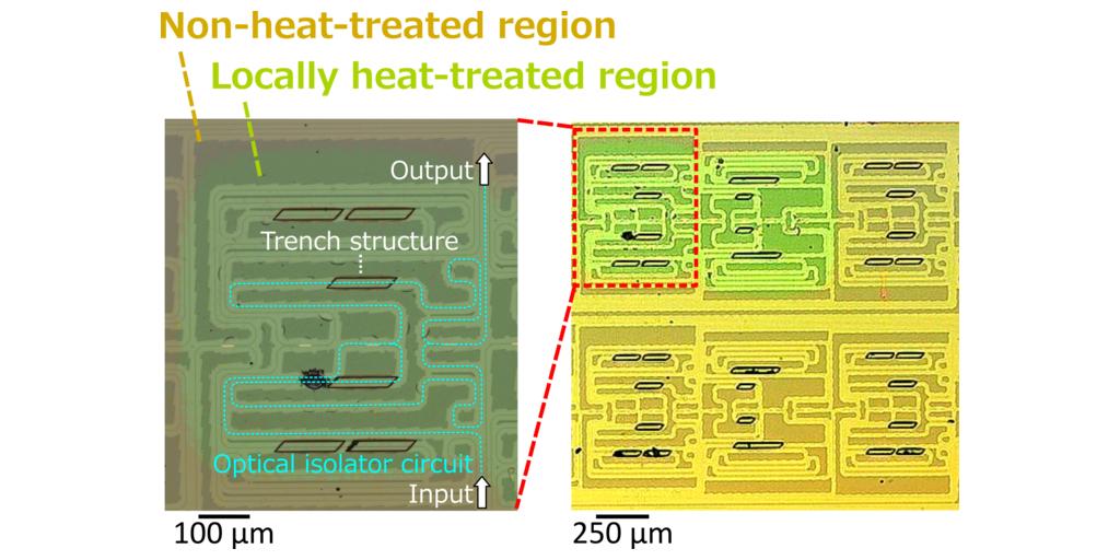



Isolator-integrated photonics chip reduces back-reflected light approximately 95%, enabling faster, energy-efficient AI data centers
KYOTO, Japan: Kyocera Corporation (President: Shiro Sakushima; "Kyocera") and the Research Institute of Electrical Communication (RIEC), Tohoku University (Director: Kazushi Ishiyama; "Tohoku University") have developed a new technology*1 for integrating optical isolators onto silicon photonics chips using "laser annealing," a localized, laser-based heat-treatment method.
An optical isolator is a component that stabilizes optical communication by allowing optical signals to be transmitted in only one direction, reducing signal reflection.
A paper summarizing these results was published on Sep. 2, 2026, in "IEEE Access," an academic journal issued by the Institute of Electrical and Electronics Engineers (IEEE).
*1 | For technology that integrates an optical isolator into a silicon photonics circuit using a laser annealing method; according to Kyocera research, July 2026. |
Development Background
As generative AI and related technologies place unprecedented demand on global data networks, silicon photonics*2 offers a solution for faster and more energy-efficient data centers. The expansion of silicon photonics is fueling demand for technologies enabling Co-Packaged Optics (CPO), which integrate optical and electronic circuits within the same semiconductor package to minimize signal paths, signal loss and power consumption.
In optical circuits, light reflected back into the laser light source degrades performance. Optical isolators, which suppress reflected light, can overcome this challenge. The next generation of compact, integrated optical circuits incorporating CPO technology will require optical isolators that can be fabricated directly onto silicon photonics chips.
Optical isolators typically use a crystalline material known as “magneto-optical garnet.” To function as an optical isolator, this material requires heat treatment at approximately 600°C or higher. However, heating the entire silicon photonics chip to this temperature can damage electrodes, wiring and other on-chip elements. Finding a way to selectively heat-treat only the magneto-optical garnet without overheating other areas of the chip has remained a significant challenge.
To address this challenge, Kyocera and Tohoku University developed a monolithic integration technology*3 that directly fabricates optical isolators onto silicon photonics chips through a “laser annealing” process, in which a laser beam is applied locally to the areas of the chip requiring heat treatment. Kyocera and Tohoku University demonstrated the device’s operation.
*2 | Silicon photonics: A technology that forms optical circuits on silicon, a semiconductor material, and uses optical instead of electrical signals to transmit and process information. |
*3 | Monolithic integration technology: A technology that integrally forms multiple functional elements on the same substrate. |
Features
1) Localized laser heating enables heat treatment of magneto-optical garnet without damaging the silicon photonics chip
A near-infrared laser beam is applied only to an optical isolator circuit region measuring approximately 700x700 microns (μm), where the magneto-optical garnet film has been deposited, causing it to crystallize with the properties needed to suppress reflected light. Unlike conventional methods that heat the entire chip in a furnace, this approach virtually eliminates thermal impact on the surrounding optical circuits and electrodes.
2) Optical isolator test on silicon photonics chip
Using this technology, the research team fabricated a device with a structure that utilizes light interference and experimentally demonstrated its operation as an optical isolator. In the experiment, the team compared the optical output corresponding to signal light, or forward propagation, with that corresponding to back-reflected light, or backward propagation. The results confirmed an isolation ratio of 13.6 dB in the optical communication wavelength range, reducing back-reflected light by approximately 95%. Electron microscopy also confirmed that the magneto-optical garnet in the laser-irradiated area had crystallized well on the silicon waveguide.
Future Development
Kyocera and Tohoku University have previously worked together to develop related optical isolator technologies that can be integrated onto optical circuits*4. To commercialize these technologies, the two organizations aim to achieve even lower loss, higher efficiency and improved productivity for mass production. They will continue to advance their collaboration and contribute to the development of an efficient and sustainable information society.
*4 | Prior joint research result (T. Sugita et al., “Nanocomposite Garnet-Enabled Monolithically Integrated Magneto-Optical Isolator Using an Asymmetric Mach–Zehnder Interferometer,” ACS Appl. Opt. Mater., vol. 4, no. 6, pp. 1813–1820, Jun. 2026, doi: 10.1021/acsaom.6c00176). |
Paper Information
Journal: IEEE Access
Title: Monolithic Magneto-Optical Mach–Zehnder Isolator Using Laser-Annealed Iron Garnet on a Silicon Waveguide
Authors: Tomoya Sugita, Reona Motoji, Yuki Yoshihara, Dan Maeda, Hiroki Yamamoto, Hibiki Miyashita, Kazushi Ishiyama, Taichi Goto
DOI: 10.1109/ACCESS.2026.3729586 (https://doi.org/10.1109/ACCESS.2026.3729586)
- IEEE is a registered trademark of The Institute of Electrical and Electronics Engineers, Incorporated.
Fonte: Business Wire
Related news

Last News
RSA at Cybertech Europe 2024
Alaa Abdul Nabi, Vice President, Sales International at RSA presents the innovations the vendor brings to Cybertech as part of a passwordless vision for…
Italian Security Awards 2024: G11 Media honours the best of Italian cybersecurity
G11 Media's SecurityOpenLab magazine rewards excellence in cybersecurity: the best vendors based on user votes
How Austria is making its AI ecosystem grow
Always keeping an European perspective, Austria has developed a thriving AI ecosystem that now can attract talents and companies from other countries
Sparkle and Telsy test Quantum Key Distribution in practice
Successfully completing a Proof of Concept implementation in Athens, the two Italian companies prove that QKD can be easily implemented also in pre-existing…
Most read
Datavault AI to Participate in Lake Street Capital Markets 10th Annual…
Datavault AI Inc. (“Datavault AI” or the “Company”) (Nasdaq: DVLT), an Artificial Intelligence Platform (“AIP”) company focused on transforming data and…
Elastic Brings OpenAI GPT Cyber Models Into Elastic Security to Help Defenders…
Elastic (NYSE: ESTC) today announced plans to bring OpenAI GPT cyber models into Elastic Security. By integrating these models directly into Elastic Security…
CoreWeave to Participate in the Goldman Sachs Communacopia + Technology…
CoreWeave Inc. (Nasdaq: CRWV), The Essential Cloud for AI™, today announced that Michael Intrator, Co-Founder, CEO and Chairman of the Board, will present…
CauzzyAI and Unilever Prestige Partner to Accelerate AI Innovation Across…
#ai--CauzzyAI (cauzzy.ai) today announced a strategic partnership with Unilever Prestige, bringing its Enterprise AI platform within the Unilever Prestige…
G11 Media Networks
InnovationOpenLab is a channel of BitCity, a newspaper registered at the court of Como ,
n. 21/2007 del
11/10/2007- Registration ROC n. 15698
G11 MEDIA S.R.L.
Registered office Via NUOVA VALASSINA, 4 22046 MERONE (CO) - P.IVA/C.F.03062910132
Como business register n. 03062910132 - REA n. 293834 CAPITALE SOCIALE Euro 30.000 i.v.